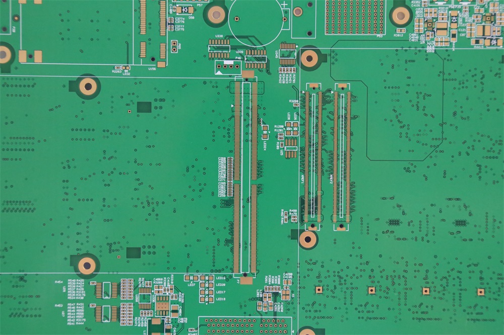
In the process of designing high speed PCB circuit board, seemingly simple via holes that leave no sound are likely to bring significant negative effects to the circuit board. Today, Weifu Precision Manufacturer will talk to you about how to reduce the adverse effects of parasitic effects in through-hole design in high speed PCB circuit board: 1. The pins of the power supply and ground should be perforated nearby, and the shorter the lead between the vias and pins, the better, as they can lead to an increase in inductance. At the same time, the leads of the power and ground should be as thick as possible to reduce impedance. 2. The signal routing on the PCB circuit board should be minimized by not changing layers, which means unnecessary through holes should be avoided as much as possible. 3. The use of thinner PCB circuit board is beneficial for reducing the two parasitic parameters of via. 4. Considering both cost and signal quality, choose a reasonable size for the through-hole. For example, for the design of 6-10 layer memory module PCB circuit board, it is better to use 10/20Mil (drilled/soldered) through holes. For some high density small-sized boards, 8/18Mil through holes can also be used. Under current technological conditions, it is difficult to use smaller through-holes. For the via of the power or ground wire, larger sizes can be considered to reduce impedance. 5. Place some grounded vias near the vias of the signal switching layer to provide the nearest circuit for the signal. Even a large number of extra grounding vias can be placed on the multi layer PCB. Of course, flexibility and versatility are also required during design. The through-hole model discussed earlier refers to the situation where each layer has solder pads, and sometimes we can reduce or even remove the solder pads of certain layers. Especially in cases where the through-hole density is very high, it may lead to the formation of a groove in the copper layer that separates the circuit. To solve this problem, besides moving the position of the through-hole, we can also consider reducing the size of the solder pad in the copper layer. By reading the above content, I believe everyone has gained some understanding of through-hole design in high-speed printed circuit board. Weifu Precision has shared this with you. If you want to learn more related information, you can consult our customer service personnel online or visit Weifu's official website